
Mass Production Breakthrough of Automotive Backlight Mini/Micro LED: Process Bottlenecks of MIP Route & Flip Chip Bonding Solutions
2026-07-31(365)Browse
As smart cockpits evolve toward larger screens, superior image quality and lower power consumption, automotive backlight technology is rapidly upgrading from Mini LED to Mini/Micro LED. The number of dimming zones has jumped from hundreds to thousands, imposing stringent automotive-grade requirements on pixel density, luminance uniformity and long-term reliability. Industry statistics show that the global automotive Mini/Micro LED backlight market size will exceed USD 1.2 billion in 2026, with a compound annual growth rate (CAGR) exceeding 85% in the next five years. It stands out as one of the most high-growth, high-certainty segments in the advanced display industry.
Selection of Automotive Display Routes: MIP Packaging Meets Automotive-Grade Mass Production Requirements
Two mainstream technical routes are available for Mini/Micro LED backlights: COB direct mounting and MIP integrated packaging.
The COB solution suffers limited integration potential. The pick-and-place process for discrete bare chips features narrow process windows, high difficulty in large substrate fabrication, expensive post-sales maintenance, and insufficient vibration and temperature resistance for long-term in-vehicle operation.
MIP pre-integrates RGB chips into a single pixel device, enabling one-step mounting and drastically lowering precision thresholds for substrate processing. Its packaging shell comes with built-in moisture-proof and impact-resistant protection, fully complying with automotive reliability standards, and has become the dominant commercialized solution for automotive backlights.
However, MIP paired with traditional face-up chip bonding faces two inherent mass production bottlenecks that cannot be fundamentally eliminated: yield defects caused by pin piercing on chips, and optical uniformity defects arising from segmented processing of large substrates.
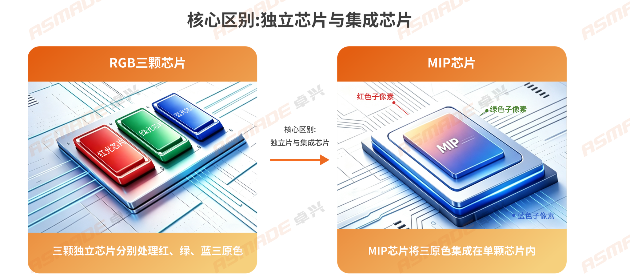
Left side: Three independent RGB chips, each handling red, green and blue primary colors separately.
Right side: MIP integrated chip that embeds red, green and blue sub-pixels into a single die.
Core distinction: Discrete separate chips vs monolithic integrated chip.
Piercing Hazards of Face-Up Chip Bonding Directly Conflict with Automotive "Zero Failure" Standards
Automotive backlight chips operate continuously under harsh conditions including alternating high/low temperatures and vibration shocks. The integrity of electrode structures directly determines device service life. In conventional face-up bonding, ejector pins press directly against the chip electrode surface. Micro-scale metal electrodes are prone to indentation and hidden cracks under pressure. Some of these damages cannot be detected during factory inspection, yet they gradually develop into electrode open circuits and dead pixels after prolonged vehicle operation, severely compromising product reliability.
Industry test data indicates that for 0306-format MIP devices manufactured via face-up bonding, physical electrode damage accounts for 20%~30% of total defective products. When deployed in automotive applications, such latent defects lead to excessive after-sales costs and safety risks, creating a fundamental conflict with the automotive-grade "zero defect" quality target. Tuning pin parameters or replacing pin materials alone cannot eliminate this issue at its source.
Flip Chip Bonding Technology: Resolve Automotive-Grade Mass Production Difficulties via Force Bearing Mechanism Redesign
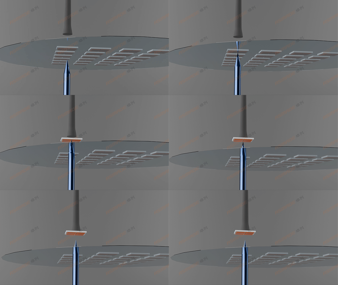
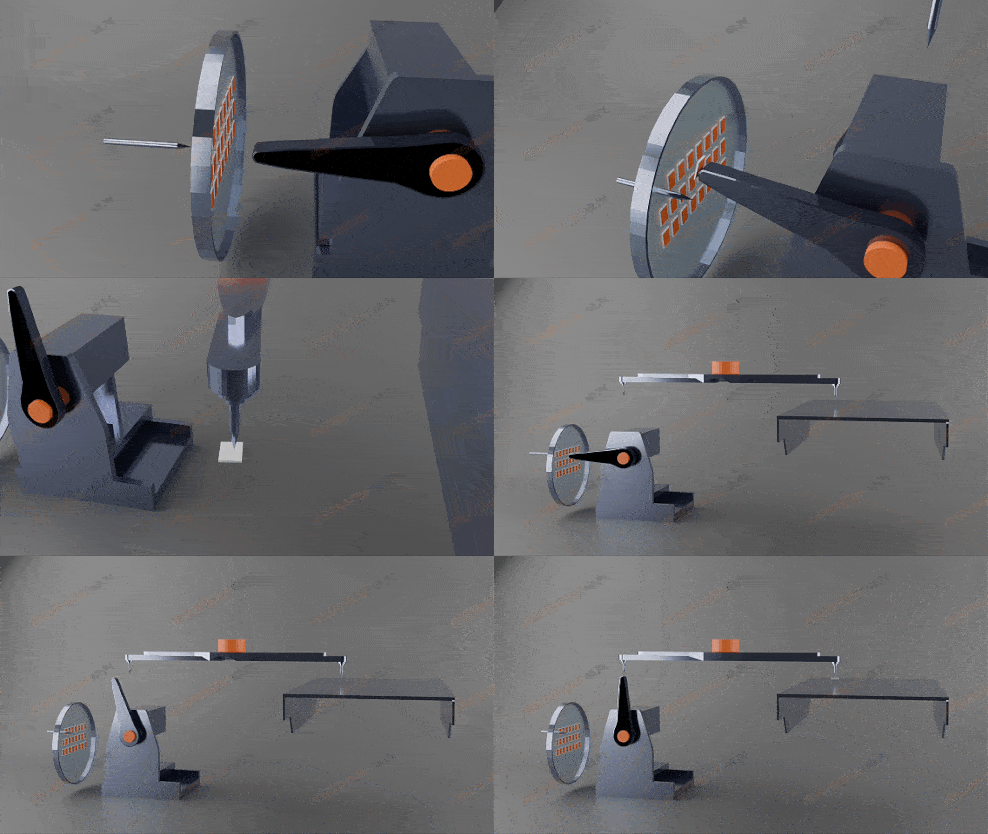
The core logic of flip chip bonding lies in reconstructing the force-bearing surface of the die: a servo flipping mechanism shifts the contact surface of ejector pins from the fragile electrode side to the high-hardness sapphire substrate side. This fundamentally eradicates electrode damage at the physical contact source, while retaining the cost-effectiveness and high flexibility of standard blue films, perfectly aligning with the comprehensive quality, cost and efficiency demands of automotive MIP mass production.
Inherent Zero Piercing Damage to Underpin Automotive-Grade Reliability
Sapphire substrates reach a Mohs hardness of 9, delivering far superior mechanical shock resistance compared to micro-thin metal electrodes. During flip chip bonding, ejector pins only contact the sapphire substrate, while the entire electrode surface remains suspended with zero contact and zero force exposure. This prevents electrode indentation, breakage, metal contamination and lattice microcracks induced by ejector pins, eliminating the top source of physical damage defects in the bonding process from the root mechanism.
For automotive scenarios, this guarantees complete structural integrity of pixel electrodes, drastically lowering long-term failure risks, and reduces chip damage rates in the bonding process to nearly zero, fully satisfying the bottom-line automotive "zero defect" quality requirements.
Three Structural Mass Production Drawbacks Brought by Segmented Multi-Panel Processing
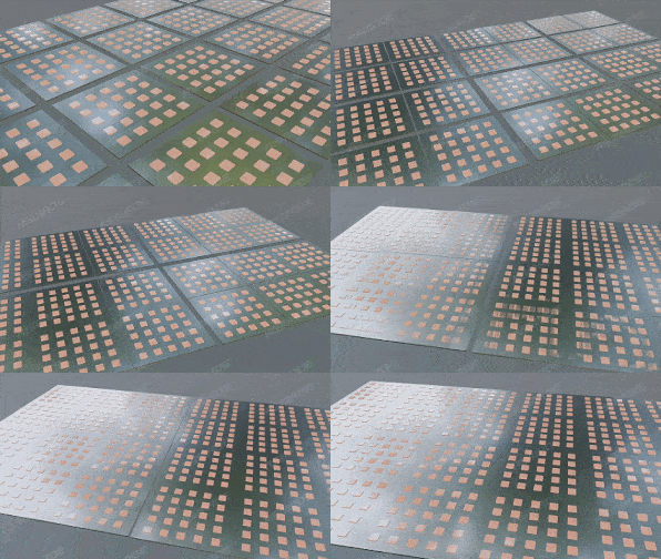
Conventional mainstream bonding equipment is limited by processing frame size. A standard 600×337.5mm 16:9 automotive backlight cabinet must be split into 12 or even 24 separate panels for batch bonding, triggering three unavoidable issues:
Image quality defects: Physical gaps formed by substrate segmentation create fixed dark lines and bright bands, resulting in disjointed visuals when viewed at close range inside the vehicle and degrading premium cockpit visual experience.
Substandard luminance uniformity: Attenuated solder paste activity, drifting equipment parameters and fluctuating ambient temperature/humidity across segmented batches easily push luminance deviation beyond the automotive ±3% uniformity threshold. Enterprises must add extra luminance correction procedures, raising overall manufacturing costs.
Long-term reliability hazards: Segmentation joints form stress concentration points, which lead to pad cracking and pixel detachment under prolonged vehicle vibration and thermal cycling, failing to meet automotive long-lifetime design standards.
Zhuoxing AS3606 Extra-Large Single-Sheet Bonding Machine Eliminates All Pain Points of Segmented Processing in One Step
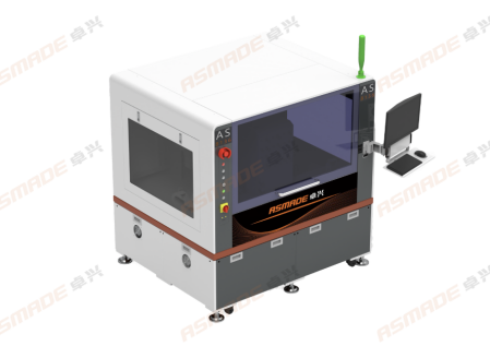
To address widespread industry pain points of segmented processing, the Zhuoxing AS3606 flip chip bonder features an ultra-large bonding frame of 620×350mm, fully compatible with the standard 600×337.5mm 16:9 backlight cabinet widely adopted across the industry. It enables one-shot full-sheet bonding for an entire substrate, eliminating the need to split work into 12 or 24 segmented batches as with mainstream industry solutions. This breakthrough from 24 segmented panels to 1 single integrated sheet fundamentally resolves uniformity challenges at the hardware level, delivering four quantifiable mass production benefits:
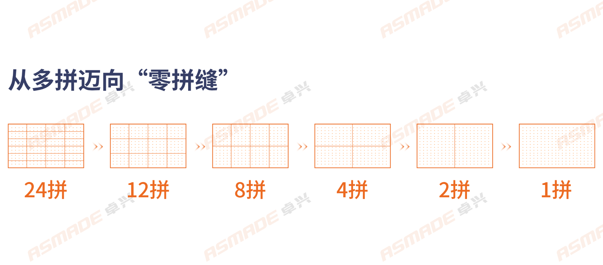
1. Integrated imaging for "zero-seam" picture quality
Continuous pixel arrays cover the entire substrate without segmentation-induced bright/dark bands, delivering smooth gradient transitions for backlight dimming zones. It is especially suitable for large-size center control and co-pilot entertainment screens viewed at short distances inside vehicles, achieving generational improvements in picture integrity and fineness.
2. Synchronized single-sheet bonding optimizes processes to cut costs and boost efficiency
The full substrate undergoes complete bonding within one workstation and one solder paste activity cycle, stably meeting automotive luminance uniformity metrics. Redundant optical correction steps for segmented panels are removed, lowering overall manufacturing costs per backlight board.
3. Shortened production cycle and improved direct yield
Eliminating repeated loading/unloading, substrate transfer and re-alignment steps required for segmented processing cuts production cycle time by 60% compared to the 12-panel segmented scheme. It also reduces risks of substrate damage and particle contamination from repeated handling, significantly lifting the direct bonding yield.
Elimination of segmentation stress to match automotive long-lifetime standards
Integrated single-sheet forming removes stress concentration zones, delivering consistent pixel bonding across the entire board. Pad stability is greatly enhanced under extreme temperature swings and continuous vibration, drastically reducing pixel failure rates over long-term service.
Automotive-Oriented Adaptation of Zhuoxing AS3606 Flip Chip Bonder
Integrating two core capabilities – flip die handling and ultra-large single-sheet bonding – the Zhuoxing AS3606 flip chip bonder targets two universal industry bottlenecks in automotive MIP mass production. Its servo flipping mechanism restructures die force-bearing design to fundamentally avoid electrode piercing defects from face-up processes, stably guaranteeing automotive-grade chip yield and long-term reliability. Supported by its 620×350mm ultra-large bonding frame, the machine completes processing for standard 600×337.5mm 16:9 backlight cabinets in a single pass, thoroughly erasing segmentation-induced defects such as dark lines and inconsistent luminance/chromaticity. The equipment systematically removes mass production bottlenecks of automotive backlights from both chip and substrate perspectives, with deep customization for strict automotive process standards to translate its zero-damage, high-flexibility and high-uniformity process advantages into stable mass production capacity.
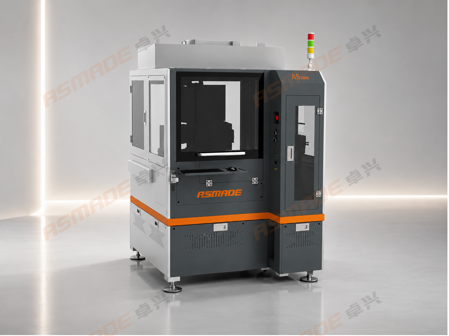
Core Process: Zero Piercing Damage & High Precision to Meet Automotive Quality Specifications
The AS3606 adopts side pick-up and high-precision servo flipping mechanisms, with ejector pins solely contacting the sapphire substrate side. Both rigid and flexible ejector pins are optional to completely eliminate electrode piercing damage at the source. Paired with bottom high-speed vision scanning and real-time XYθ compensation, it achieves a mounting precision of ±15μm and angular error ≤2°, balancing zero damage and uniform mounting consistency to satisfy automotive high-precision placement standards.
Production Line Flexibility: Compatible with Mass Mixed Production of Multi-Specification Backlights
The machine natively supports mixed bonding of single-color 12-ring and RGB 5-ring wafers without pre-sorting. Intelligent path programming enables rapid switching between multi-specification chips, boosting model changeover efficiency by over 60%. Equipped with a 15-layer wafer ring storage module and non-stop ring replacement design, it sustains high equipment utilization rates to match high-volume stable automotive production rhythms.
Production Line Compatibility: Seamless Integration with Existing Digital Automotive Manufacturing Lines
It supports multiple automatic line layouts including right-in right-out and left-in right-out, enabling direct docking with existing production lines without large-scale factory reconstruction. Deep compatibility with factory MES systems realizes full-process traceability of process parameters, real-time equipment status monitoring and intelligent production scheduling, complying with automotive manufacturing regulations requiring full-lifecycle traceability.
Automotive Mini/Micro LED backlight is currently in the stage of large-scale mass production breakthrough. Market penetration of the MIP route is determined by three core factors: production line yield, optical uniformity and comprehensive manufacturing costs. Flip chip bonding resolves yield bottlenecks from face-up piercing damage via force-bearing mechanism redesign, while ultra-large single-sheet bonding eliminates image quality, uniformity and reliability defects caused by segmented processing at the hardware level. The combined process has become a highly competitive core manufacturing route for standardized mass production of automotive MIP backlights. The Zhuoxing AS3606 flip chip bonder solution empowers display packaging manufacturers to build automotive-compliant backlight production lines and accelerate the large-scale commercialization of automotive Mini/Micro LED backlights.
About Us
Shenzhen Asmade Semiconductor Technology Co., Ltd. is a national-level "Little Giant" specialized, sophisticated, unique and innovative enterprise focusing on advanced packaging equipment.
Founded by a team of world-leading motion control and packaging experts, the company boasts 20 years of profound technical accumulation and market application experience. Its core business covers advanced display, AI devices and PLP panel-level packaging equipment, alongside a complete product portfolio including power device packaging, intelligent control equipment and packaging process management systems.
Committed to delivering one-stop, high-performance and high-reliability advanced packaging solutions to global clients, we are a high-tech enterprise integrating R&D, design, manufacturing, sales and technical services.
New Information
-
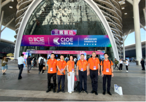
Highlights|ASMADE · Zhuoxing Semiconductor at CIOE 2026 — The 27th China International Optoelectronic Exposition
On September 11, 2026, the three day 27th China International...
-
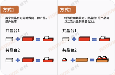
AS8138 High Precision Eutectic Bonder|Dual Eutectic Stage Architecture Innovation to Solve Mass Production Challenges of Multi Layer Stacking for High Speed Optical Devices
https://weixin.qq.com/sph/ANb7T2gnxp(点击链接播放视频) Dri...
-
Cordially Invited | ASMADE Zhuoxing Semiconductor Meets You at CIOE 2026 — The 27th China International Optoelectronic Exposition
Cordially Invited | ASMADE Zhuoxing Semiconductor Meets You ...
-
Mass Production Breakthrough of Automotive Backlight Mini/Micro LED: Process Bottlenecks of MIP Route & Flip Chip Bonding Solutions
As smart cockpits evolve toward larger sizes and higher imag...
0755-29691921
Hotline:0755-29691921
Phone:0755-29691921
Fax:0755-29691921
Email:market@asmade.cn
Address:Building 3, Xifengcheng Industrial Park, Fuhai Street, Bao'an District, Shenzhen City, Guangdong Province




 0755-29691921