
Flip Chip Bonding: Core Process to Break Through Mass Production Yield Bottlenecks of Micro LED MIP
2026-07-24(472)Browse
According to the back-end equipment industry report released by Yole Group in July 2026, the global market size of semiconductor post-packaging equipment will reach USD 9.5 billion for the whole year. Among them, the five-year compound annual growth rate of Micro LED chip shipments hits 132.4%. The industry is rapidly moving past laboratory verification and entering the stage of large-scale mass production. In the terminal manufacturing cost structure, the die bonding process accounts for more than 45% of total costs, directly determining the yield, production capacity and commercialization pace of the entire production line. It serves as the core bottleneck for mass production of new displays.
Two mainstream process routes have taken shape in the industry, showing differentiated performance under different pixel pitch scenarios: the COB route for pitches above P0.6 is mature and controllable, with remarkable advantages in integration and overall cost for full-panel die bonding. However, when moving to sub-P0.6 fine-pitch segments, chip sizes keep shrinking, and the drawbacks of the COB route become prominent rapidly. The separate mounting process for three RGB chips leads to exponentially higher precision requirements for PCB wiring. Large substrates have to be split into multiple panels for processing, resulting in uneven brightness and color, reduced yield and narrowed process windows. The technology has nearly hit its fundamental theoretical ceiling.
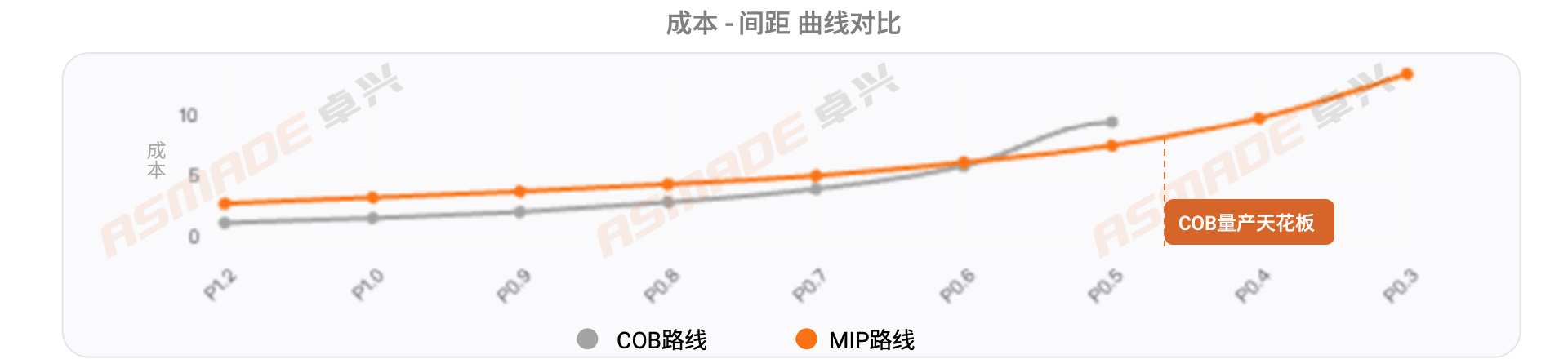
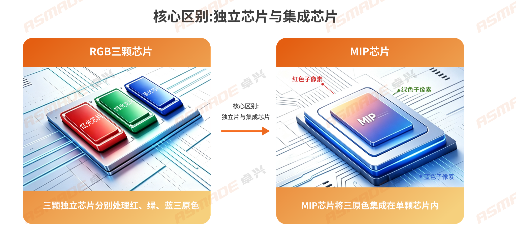
Against this backdrop, MIP packaging has become the core route for mass production of fine-pitch products. It pre-integrates RGB chips into a single pixel device for one-step mounting, greatly relaxing process requirements from a physical perspective and effectively lowering precision pressure on PCBs and die bonding. Nevertheless, when MIP adopts traditional forward die bonding processes, ejector pins directly act on the chip electrode surface. Physical damage defects account for 20%~30% of total defects in production of 0306 and smaller chip sizes. Such defects are fundamental flaws that cannot be eliminated merely by optimizing process parameters, emerging as the key bottleneck restricting MIP yield improvement.
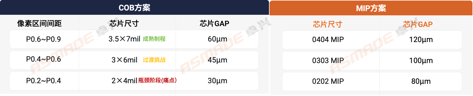
The industry urgently needs to restructure die bonding solutions from the perspective of force-bearing mechanisms, giving rise to the flip chip bonding process equipped with die flipping mechanisms. This process shifts the force-bearing surface to the high-hardness sapphire substrate, ensuring zero contact force on the electrode surface throughout the process and fundamentally eliminating the risk of pin damage. The market has formed rigid demand for high-precision, high-throughput flip chip bonding equipment compatible with large-size substrates. Data shows that driven by the rapid expansion of the new display industry, the flip chip bonding equipment track leads the entire industry in growth momentum, with a compound annual growth rate of 42.7% in the next six years. It stands as the most definitive incremental equipment track in the mass production phase of Micro LED. It avoids compressive damage to electrodes and can adapt to both MIP packaging and direct glass substrate mounting production routes, making it the standardized optimal process for Micro LED mass production. Still, multiple challenges remain for large-scale industrial rollout.
Core Mass Production Pain Points of New Display Packaging: Structural Process Defects & Dual Supply Chain Constraints
Forward Die Bonding: Inherent Risk of Electrode Pin Damage
Forward die bonding is a mature long-standing process widely adopted across the industry, yet its structural design carries inherent quality defects that cannot be eradicated. For incoming flip chips, the sapphire substrate side faces upward while the electrode surface adheres directly to the blue tape. When ejector pins peel off chips, force penetrates the blue tape and acts directly on the fragile metal electrode layer.
From a force-bearing structural analysis, sapphire substrates feature high hardness and strong deformation resistance, whereas the metal electrode layer is only a few microns thick with extremely weak compression resistance. Concentrated stress from ejector pins easily causes electrode depressions, metal layer breakage, and even latent lattice cracks. Some of these damages cannot be identified through visual inspection and become hidden hazards for product reliability failures in later stages. Optimizing ejector pin materials, heights and speeds can only reduce damage probability, without changing the physical nature that pin force directly reaches electrodes — this is a typical fundamental theoretical defect.
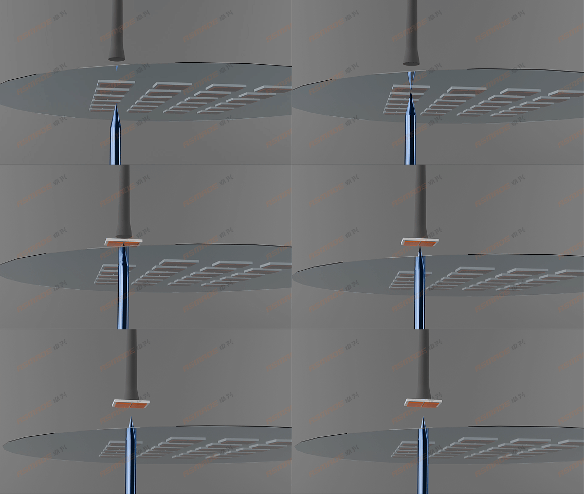
Needle Piercing Debonding Solution: Avoids Pin Damage Yet Creates New Mass Production Contradictions
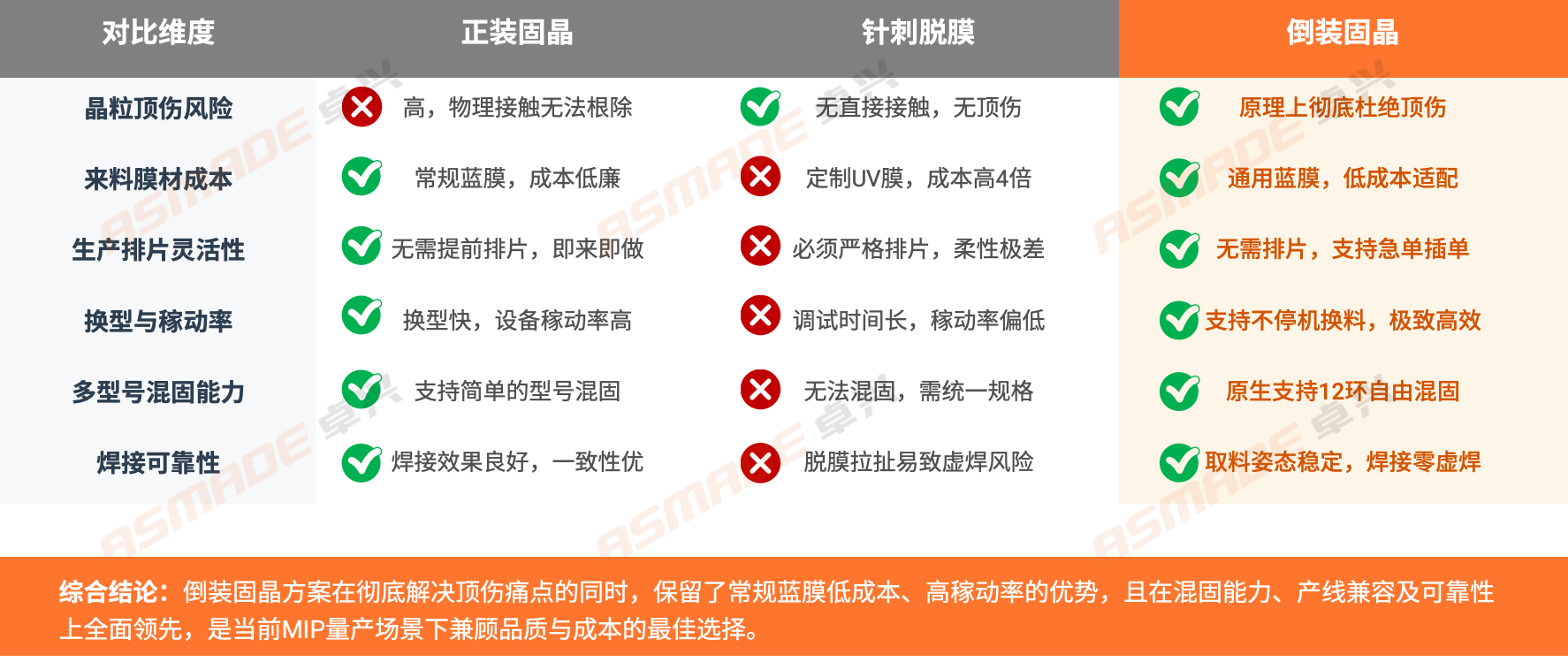
To resolve electrode pin damage, the industry developed the needle piercing debonding process. Custom UV release tapes carry chips, and arrays of piercing needles puncture the adhesive layer to separate chips, eliminating direct hard pin contact with electrodes and avoiding pin damage at the contact level.
However, this solution brings heavy costs to mass production:
1. High Consumable Costs: It relies on imported custom UV release tapes whose material cost is 4 times that of standard blue tapes. Chip manufacturers must customize incoming wafers, resulting in poor supply chain flexibility and heavy long-term consumable burdens for mass production.
2. Low Production Flexibility: Chips need pre-sorting before processing, which disables mixed die bonding of multiple models. Debugging cycles for model changeovers are lengthy for rush orders and small-batch lots, lowering equipment throughput.
3. Hidden Quality Risks: Adhesive retraction during debonding easily pulls chips and causes warpage, leading to cold joints and poor bonding during subsequent reflow soldering, introducing new reliability issues instead.
In short, needle piercing debonding only solves the single issue of pin damage while creating multiple new contradictions in cost, production flexibility and reliability, making it suboptimal for large-scale MIP mass production.
Flip Chip Bonding Process: Fundamentally Resolves MIP Yield Challenges via Packaging Route Restructuring
The core logic of flip chip bonding lies in restructuring force-bearing surfaces. A die flipping mechanism shifts ejector pin force from fragile electrode surfaces to high-hardness sapphire substrates, completely eliminating electrode damage at the root of physical contact while retaining the low-cost and high-flexibility advantages of standard blue tape processes.
Core Process Flow
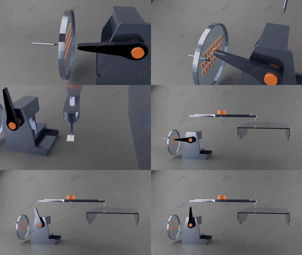
Flip chip bonding forms a closed three-step loop of "pick-up – flipping transfer – die bonding mounting" to achieve high-precision mounting with zero pin damage:
1. Wafer Pick-up: Ejector pins push chips out from the back of blue tape, with force applied entirely to sapphire substrates and zero stress on electrode surfaces. A pick-up arm vacuum-adsorbs chips via the substrate side, leaving electrode surfaces suspended without contact.
2. Wafer Transfer: The pick-up arm rotates chips 180 degrees to flip electrodes downward for mounting. High-precision servo control is built into the flipping process to guarantee chip parallelism deviation ≤0.5°, with no offset or chip dropping.
3. Die Bonding Mounting: After receiving chips, the bonding head performs position and angle compensation via high-speed bottom visual inspection, then precisely mounts chips onto substrate pads. Electrode surfaces remain free of any hard contact throughout the whole process.
Core Process Advantages
1. Fundamental Zero Pin Damage, Underlying Support for Yield Improvement Sapphire substrates reach Mohs hardness 9, far exceeding metal electrode layers in mechanical impact resistance. Ejector pin stress is evenly dispersed by substrates, preventing electrode depressions, breakage, metal contamination and latent lattice cracks caused by pin contact. It eliminates the highest proportion of physical damage defects in die bonding from the mechanism, driving chip damage rate in the die bonding process close to zero, directly lifting production first-pass yield and cutting rework & failure costs in downstream stages.
2. Compatible with Standard Blue Tape, Remarkably Optimized Mass Production Costs No custom UV release tapes are required; the process fully adapts to industry-standard general blue tape for incoming wafers. Consumable costs match forward die bonding and stand at only 1/4 of the needle piercing debonding solution. Pre-sorting steps are eliminated, enabling direct production upon chip arrival, simplifying material management and process flows to further reduce operating costs.
3. Natively Supports Flexible Mixed Production, Fits Multi-Spec Manufacturing Unrestricted by pre-sorting, flip chip bonding natively supports mixed die bonding of multiple wafer rings, enabling free combination of 12 monochrome rings or 5 RGB three-color rings. Paired with intelligent random path programming, it rapidly responds to multi-model, small-batch orders with short changeover time and high equipment throughput, perfectly matching the multi-spec parallel production characteristics of the current display industry.
4. Stable Pick-up Posture, Superior Soldering Reliability Compared with the pulling-style separation of needle piercing debonding, the vacuum adsorption pick-up + servo flipping workflow of flip chip bonding delivers stable chip posture without warpage or displacement. Electrodes fit flat against pads after mounting, drastically reducing cold joints and offset soldering during reflow, delivering superior long-term product reliability.
Mass Production Rollout: From Process Principles to Production Line Adaptation
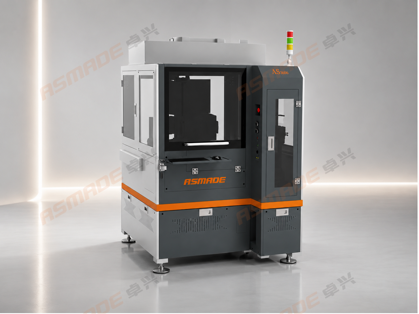
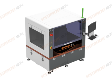
The value of process technology can only be realized through mass production rollout. Asmade Semiconductor’s AS3606 flip chip bonder dedicated to MIP boasts full-scale deployment capabilities for flip chip bonding solutions in terms of large substrate compatibility, production line interconnection and intelligent manufacturing.
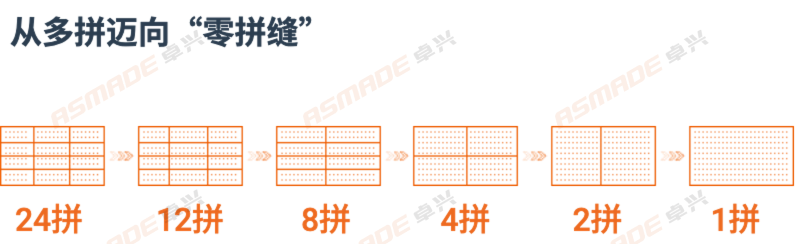
Full-Panel Die Bonding for Large Substrates: Eliminate Splitting Seams and Improve Uniformity
The AS3606 flip chip bonder from Asmade Semiconductor supports substrates up to 620×350mm, perfectly matching the industry-standard 16:9 cabinet (600×337.5mm). It enables one-step full-panel die bonding for single cabinets without splitting substrates into multiple panels for separate processing. On one hand, full-panel processing removes physical splitting seams to deliver more complete and delicate display images. On the other hand, it eliminates uneven brightness and color caused by multi-panel processing, greatly shortening the production cycle of single substrates and boosting overall output efficiency.
High-Flexibility Production Line Design for Large-Scale Mass Production Rhythms
Asmade Semiconductor AS3606 flip chip bonder natively supports mixed die bonding of 12 monochrome wafer rings and 5 RGB three-color wafer rings without pre-sorting. Combined with intelligent random path programming, it can rapidly fulfill multi-variety and small-batch orders.
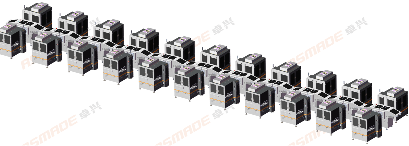
Equipped with a 15-layer wafer ring storage bin and non-stop ring replacement design, as well as a built-in angle pre-correction function, the machine enables material switching without production interruption, drastically cutting downtime caused by equipment alarms and delivering far higher equipment utilization rate than traditional solutions. Multiple units can be connected in parallel to quickly build mass production lines with a monthly capacity of tens of thousands of panels.
Full-Dimensional Production Line Compatibility, Adaptable to Factory Automation Systems
Asmade Semiconductor AS3606 flip chip bonder accurately addresses critical mass production bottlenecks:
Flexible Layout: Compatible with multiple inline connection modes including right-in & right-out, left-in & right-out, right-in & left-out. It seamlessly integrates with existing production line layouts without large-scale reconstruction.
System Interconnection: Deeply connects with factory MES systems to realize intelligent scheduling of production plans, real-time monitoring of equipment status, traceability of process parameters and data analysis.
Expandable Compatibility: Supports automatic loading and unloading via retrofitted rear-end robotic arms, meeting the upgrading demands of flexible manufacturing lines.
From the perspective of industrial evolution, the maturity of flip chip bonding is not merely an iteration of a single device, but a restructuring of the underlying logic of MIP manufacturing. Through mechanism-level innovation, it addresses the long-standing industry pain point of low yield arising from pin damage. With compatibility for standard blue tape and high-flexibility mixed production, it strikes a balance between product quality and mass production costs, laying a solid process foundation for the large-scale commercialization of the MIP route.
With the launch and application of domestic high-end equipment such as the AS3606, flip chip bonding will further accelerate the Micro LED industry’s leap from engineering trial production to large-scale manufacturing. It will speed up the penetration of new display technologies in commercial display, cinema, outdoor and other application scenarios. Together with the COB route, it will continuously drive the industry toward higher pixel density and lower manufacturing costs.
About Us
Shenzhen Asmade Semiconductor Technology Co., Ltd. is a national-level specialized, sophisticated, unique & innovative "Little Giant" enterprise deeply engaged in advanced packaging equipment and core semiconductor packaging technologies.
Founded by world-leading experts in motion control and packaging, the company boasts 20 years of profound technical accumulation and market implementation experience. Its core businesses cover new display, AI device and PLP panel-level packaging equipment, alongside a complete product portfolio including power device packaging, intelligent control equipment and packaging process management systems.
Committed to delivering one-stop, high-performance and highly reliable advanced packaging solutions for global customers, it is a high-tech enterprise integrating R&D, design, manufacturing, sales and technical services.
New Information
-
Highlights|ASMADE · Zhuoxing Semiconductor at CIOE 2026 — The 27th China International Optoelectronic Exposition
On September 11, 2026, the three day 27th China International...
-
AS8138 High Precision Eutectic Bonder|Dual Eutectic Stage Architecture Innovation to Solve Mass Production Challenges of Multi Layer Stacking for High Speed Optical Devices
https://weixin.qq.com/sph/ANb7T2gnxp(点击链接播放视频) Dri...
-
Cordially Invited | ASMADE Zhuoxing Semiconductor Meets You at CIOE 2026 — The 27th China International Optoelectronic Exposition
Cordially Invited | ASMADE Zhuoxing Semiconductor Meets You ...
-
Mass Production Breakthrough of Automotive Backlight Mini/Micro LED: Process Bottlenecks of MIP Route & Flip Chip Bonding Solutions
As smart cockpits evolve toward larger sizes and higher imag...
0755-29691921
Hotline:0755-29691921
Phone:0755-29691921
Fax:0755-29691921
Email:market@asmade.cn
Address:Building 3, Xifengcheng Industrial Park, Fuhai Street, Bao'an District, Shenzhen City, Guangdong Province





 0755-29691921