 Technology Limited")
AI Computing Power Surges: Domestic Micron-Level Die Bonder Solves High-Speed Optical Module Packaging Bottlenecks
2026-05-20(104)Browse
Revised up by 50%! Multiple authoritative institutions forecast that the global chip market will exceed $1.5 trillion by 2030, with optical modules standing as one of the fastest-growing and most technologically dynamic segments.
Driven by the explosive growth of AI computing power demand, large-scale training and inference needs have accelerated data center construction. As the core transmission medium for computing cluster interconnection, high-speed optical modules have become an essential component of AI infrastructure, ushering in robust, certain market growth. Products are evolving toward miniaturization, high density, and high-precision integration, pushing semiconductor packaging processes and equipment into a new upgrade cycle.
Large AI models generate EB-scale data traffic, rendering traditional 400G products incapable of meeting bandwidth requirements. The industry is rapidly upgrading from 800G to 1.6T. Computing cluster interconnection presents three major trends: increased port density, doubled single-channel rate, and miniaturization of optoelectronic devices. This has directly raised the bar for high-precision, highly compatible, and highly stable packaging equipment in the packaging manufacturing sector.
Traditional die bonding equipment suffers from critical pain points that severely restrict industrial development:
· Insufficient precision: Fails to meet sub-micron alignment requirements, resulting in low optical coupling efficiency and poor signal stability.
· Weak compatibility: Cannot support multi-category, multi-specification heterogeneous integration production, lacking production line flexibility.
· Poor stability: Large fluctuations in mass production yield and high costs, making it difficult to support large-order delivery.
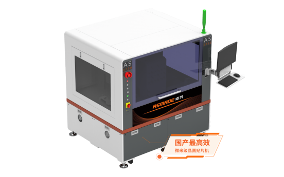
The AS8136 High-Precision Multi-Function Die Bonder by Zhuoxing Semiconductor is deeply aligned with the optical module packaging upgrade logic driven by AI computing power, providing core support for the large-scale mass production of high-end products.

Three Rigorous Requirements for High-Speed Optical Module Packaging Driven by AI Computing Power
With the accelerated rollout of AI computing infrastructure and the expansion of high-speed optical module production, packaging equipment must meet stricter performance standards:
Ultra-high die bonding precision: Satisfy precision alignment processes for miniature optoelectronic devices, ensuring product optical performance and electrical stability.
Wide-process adaptability: Support multi-architecture, multi-specification production, optimize production line configuration, and reduce equipment investment costs.
High-load stable mass production: Deliver controllable yield and stable capacity to meet industry bulk order delivery standards.
AS8136 High-Precision Multi-Function Die Bonder: Core Solution for High-Speed Optical Module Packaging
Built on precision motion control and high-precision visual positioning systems, the AS8136 addresses the full-process needs of advanced packaging for high-speed optical modules driven by AI computing power across three dimensions: precision, compatibility, and mass production capability.
l Ultra-high Die Bonding Precision
Repeat positioning accuracy: 0.5 μmXY ,bonding accuracy: ±3 μm,Angle error: ≤0.1° Meets sub-micron die bonding requirements for miniature components and high-density substrates, guaranteeing optical coupling efficiency and signal integrity under high bandwidth.
l Adaptable to High-Density Heterogeneous Integration
Compatible with packaging for optical modules, LiDAR, sensors, SiP, Chiplet, and more. Supports chip sizes ranging from 6×6 mil to 400×400 mil, accommodating iterative production of multi-architecture, multi-specification computing hardware and enhancing production line flexibility.
l Enabling Large-Scale Capacity Release
Maximum production cycle: 12,000 pieces per hour. With a mature architecture and stable yield, it effectively controls yield loss, ensures efficient delivery for high-volume, standardized mass production of high-speed optical modules, and reduces the cost of computing infrastructure construction.
The expansion of AI computing power sustains strong demand for optical modules, while advanced packaging capabilities define the upper limit of high-end optical module mass production. Centered on micron-level die bonding technology, the AS8136 integrates high-precision alignment, wide-category compatibility, and high-stability mass production. Combined with process upgrade demands driven by AI computing power, it builds a comprehensive competitive edge of core precision + full-scenario adaptation + efficient delivery.
With sub-micron die bonding capability and adaptability to complex processes for high-density substrates, it fully covers high-end electronic manufacturing packaging scenarios such as optical modules, LiDAR, and sensors. It precisely meets the technical requirements of AI computing infrastructure for highly integrated, highly reliable products. Meanwhile, its stable performance solidifies quality foundations, simplifies production flows, lowers mass production thresholds, and provides efficient, integrated die bonding solutions for enterprises of all scales.
About Us
Shenzhen Zhuoxing Semiconductor Technology Co., Ltd. is a national-level Specialized, Sophisticated, Unique, and New "Little Giant" enterprise deeply engaged in advanced packaging equipment and focused on core semiconductor packaging technologies.
Founded by a world-leading team of motion control and packaging experts, the company boasts 20 years of profound technical expertise and market implementation experience. With core businesses in new-type display, AI device, and PLP panel-level packaging equipment, it has built a complete product portfolio covering power device packaging, intelligent control equipment, and packaging process management systems.
Committed to providing global customers with one-stop, high-performance, and high-reliability advanced packaging solutions, Zhuoxing Semiconductor is a high-tech enterprise integrating R&D, design, production, sales, and technical services.
New Information
-
Zhuoxing SpinBus360 Wireless EtherCAT Transmission |Break Free from Slip Ring Restrictions to Achieve 360° Continuous Rotation Communication
Break free from the limitations and failures of traditional ...
-
AS3606 Flip Chip Bonder | Zero Die Puncture Damage, Resolving Mass Production Bottlenecks of Micro LED MIP
We have conducted an in-depth analysis of the core pain poin...
-
Real-Time Control with Standard C! Microsecond Hard Real-Time, Rapid Solution Deployment
This article introduces the AsMotion motion control solution...
-
AI Computing Power Surges: Domestic Micron-Level Die Bonder Solves High-Speed Optical Module Packaging Bottlenecks
Zhuoxing Semiconductor, a national‑level “Specialized, Sop...
0755-29691921
Hotline:0755-29691921
Phone:0755-29691921
Fax:0755-29691921
Email:market@asmade.cn
Address:Building 3, Xifengcheng Industrial Park, Fuhai Street, Bao'an District, Shenzhen City, Guangdong Province


 0755-29691921