 Technology Limited")
On-Chip Printing | Effectively Solving Dispensing and Printing Issues in Power Device Packaging
2025-07-29(1299)Browse
In the clip bonding packaging process of power devices, dispensing on the chip is crucial for ensuring tight bonding of the clip, which in turn guarantees a stable electrical connection between the clip and the chip. Consequently, the dispensing process becomes particularly significant in applications with stringent large-signal requirements.
There are two common and optional processes in clip bonding: dispensing and printing. In practical applications, the dispensing process is often confronted with various problems. Insufficient or excessive dispensing, uneven epoxy distribution, overflow, and air bubbles are some negative influences that can cause hidden dangers in clip bonding quality. Once these problems occur, they can lead to significant product-quality accidents in downstream processes.

Focusing on the challenging problems in the industry, ASMADE researches on-chip printing technology, which is gaining prominence and demonstrating unique advantages in power semiconductor packaging. It aims to enhance the packaging yield of high-signal power devices. Utilizing flexible stencil printing, it directly prints solder paste or epoxy on the chip. This avoids issues like chip damage and uneven epoxy distribution, ensuring product performance consistency and quality stability. Applications include High-Power Diode, MOSFET, DrMOS, and Multi-Dies Clip.

On-chip printing is an advanced printing technology with high implementation difficulty.
Firstly, chip surfaces are highly sensitive to impurities. Before printing solder paste on a chip, it's essential to ensure its surface is clean and free of contaminants like oil stains and dust. Even tiny impurities can negatively impact solder paste adhesion and welding quality, potentially causing chip shorts or performance degradation.
Secondly, choosing and controlling the welding process becomes more critical once the solder paste is directly printed on the chip. Direct chip welding demands a more precise temperature curve and control of welding time. During reflow welding, if the temperature is too high or the process takes too long, the internal structure of the chip may be damaged. Conversely, if the temperature is too low or the reflow time is too short, it may result in a poor welding outcome.
Lastly, the amount of solder paste requires strict control. Excessive solder paste may cause a short circuit during welding, potentially damaging the chip. Conversely, insufficient solder paste may lead to an unstable weld or a cold joint.
Nowadays, fast-developing technology is driving chip miniaturization and high-performance enhancement. Although on-chip printing faces numerous challenges, its advantages are gradually emerging.
Stencil Printing: High Precision Mass Manufacture
Compared to chip dispensing, on-chip printing offers more precise control over the position and amount of solder paste on the chip.
Stencils accurately position solder paste on the chip. During mass production, printers efficiently apply solder paste by moving the scraper rapidly across the stencil, combining precision with speed.
Stencils, typically made from stainless steel sheets, possess high mechanical strength. Unlike softer materials used in silicone or screen printing, they resist deformation and edge-curling during repeated scarper actions, maintaining accuracy and efficiency throughout mass manufacture.
On-Chip Printing: High Demand and High Quality Manufacture
In some electronic fields with extremely high product requirements, chips with special packaging are used to take up less space on the circuit board and achieve greater circuit integration. On-chip printing technology, along with advanced clip bonder and reflow machine, can closely connect tiny chips to circuit boards, ensuring reliable electrical performance.
When packaging and integrating chips of different functions and manufacturing processes, on-chip printing can create electrical connections between chips. This allows for high-density interconnection, optimized signal paths, reduced packaging size, improved system performance, and a multi-functional integrated solution.

To achieve finer processes and higher-quality manufacturing, on-chip printing is an optimal choice. But to realize on-chip printing, it demands not only precise machine but also robust R&D capabilities.
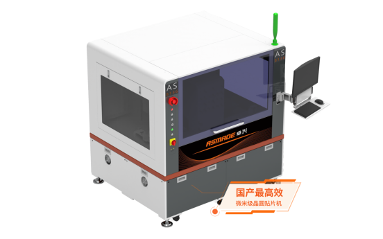
Chip-Level Printer
ASMADE pioneered the on-chip printing technology and is currently the sole company applying this technology in the industry. Besides, the Chip-Level Printer also supports functions such as narrow border printing, post-printing AOI inspection, and stencil loading/unloading without adjustment, providing a significant boost to the industry's high-speed development. It reached a position accuracy of ±0.01mm and an angular accuracy of ±0.025mm.
Also, ASMADE provides an automatic clip bonding solution including Chip-Level Printer, Clip Bonder and Formic Acid Vacuum Reflow Oven, which can handle over 100 different devices. The CLIP Bonder uses advanced clip bonding packaging technology, and the vacuum formic acid welding furnace features high air tightness and formic acid welding process, achieving a lower void rate in welding.

About Us
ASMADE (SHENZHEN) TECHNOLOGY LIMITED, a national high-tech enterprise founded by international leading motion control expert team, gathered the industry's top packaging technology experts, focusing on the research and development of high-precision semiconductor equipment, manufacturing and sales.
The main machines are semiconductor packaging equipment, power device packaging equipment, MINI LED die bond equipment, intelligent control equipment and semiconductor packaging process management system.
Dedicated to providing one-stop semiconductor packaging process die bond solutions.
New Information
-
Zhuoxing SpinBus360 Wireless EtherCAT Transmission |Break Free from Slip Ring Restrictions to Achieve 360° Continuous Rotation Communication
Break free from the limitations and failures of traditional ...
-
AS3606 Flip Chip Bonder | Zero Die Puncture Damage, Resolving Mass Production Bottlenecks of Micro LED MIP
We have conducted an in-depth analysis of the core pain poin...
-
Real-Time Control with Standard C! Microsecond Hard Real-Time, Rapid Solution Deployment
This article introduces the AsMotion motion control solution...
-
AI Computing Power Surges: Domestic Micron-Level Die Bonder Solves High-Speed Optical Module Packaging Bottlenecks
Zhuoxing Semiconductor, a national‑level “Specialized, Sop...
0755-29691921
Hotline:0755-29691921
Phone:0755-29691921
Fax:0755-29691921
Email:market@asmade.cn
Address:Building 3, Xifengcheng Industrial Park, Fuhai Street, Bao'an District, Shenzhen City, Guangdong Province


 0755-29691921