 Technology Limited")
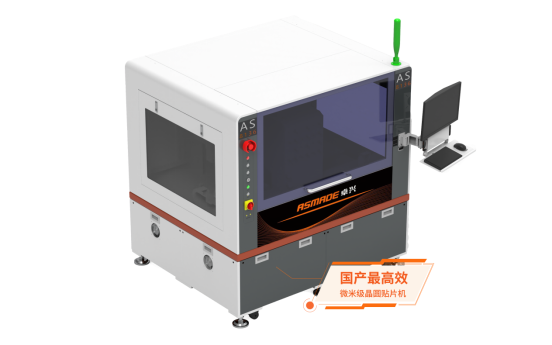
Semiconductor Epoxy Die Bonder | Combining Spot Epoxy Process with Die Bonding Process in One Machine, Capable of Handling Numerous Products.
2025-04-24(2535)Browse
The Epoxy Die Bonder is a semiconductor machine that features both the spot epoxy process and die bonding process. It can conduct spot epoxy processes and stamping processes using epoxy and other adhesives. This machine is suitable for small-signal epoxy process power devices, sensors, SIP, Chiplet, IC, MOS, and other products.

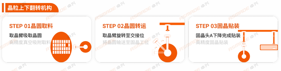
New Equipment Solution: Turret Die Bonding Mechanism
ASAMDE develops an advanced machine structure-turret die bonding mechanism, which is equipped with six single nozzles and can perform multi-process parallel operation. The machine can conduct die pickup, placement and photograph precision compensation simultaneously with the help of turret multi-station structure. This achieves non-stop die bonding and manufacture time shorten, with the efficiency improved by 60%.

Here is the standard configuration of the die bond table:

The machine also features a self-developed pressure control system by ASMADE. The motor is directly connected, enabling stable pressure control during die bonding under varying resistance. It allows dynamic pressure adjustment with a device pressure range of 30-300g (±5g).
Various Processes Adaptation: Optional Three Dispensing or Stamping Process
The machine can be equipped with three dispensing groups. It can operate the dispensing process and die bonding process simultaneously so that manufacturers don’t need to purchase separate dispensing machines. In addition to supporting dispensing process, the epoxy die bonder also accommodates stamping processes. It’s indeed a real multi-functions machine and the process structure can be easily changed.
Dispensing Features:
• Equipped with different dispensing controllers to meet diverse process requirements.
• Providing different functions like frame heating based on specific process needs.
• Visual recognition of dispensing positions and support for importing preset patterns and epoxy mappings.
Dispensing Mechanism:

Multi-material Compatibility: Different Wafer Sizes and Custom Trays
The Epoxy Die Bonder supports different wafer sizes, including 2/4/6/8/12-inch wafers. It has automatic expansion for 12-inch wafers and accommodates single 6-inch Teflon Rings, Waffle Pack, and GelPAK. Custom trays can also be made according to specific requirements.

Up Look Camera with Precision Compensation
Here are some specific parameters of the Epoxy Die Bonder: fitting X/Y accuracy ±15um, angular error ≤±1°and manufacture time 22.5k/h.
We can flexibly installs a up look camera or a transfer station at the table because of the turret structure, enabling simultaneous die bonding and precision compensation. The machine also has AI automatic precision compensation and pressure correction functions.

In the face of increasingly fierce industry competition, ASMADE is committed to providing more efficient and precise solutions for manufacturers and making dedication to the development of the semiconductor industry with advanced semiconductor packaging technology.
About Us
ASMADE (SHENZHEN) TECHNOLOGY LIMITED, a national high-tech enterprise founded by international leading motion control expert team, gathered the industry's top packaging technology experts, focusing on the research and development of high-precision semiconductor equipment, manufacturing and sales.
The main machines are semiconductor packaging equipment, power device packaging equipment, MINI LED die bond equipment, intelligent control equipment and semiconductor packaging process management system.
Dedicated to providing one-stop semiconductor packaging process die bond solutions.
New Information
-
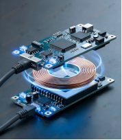
Zhuoxing SpinBus360 Wireless EtherCAT Transmission |Break Free from Slip Ring Restrictions to Achieve 360° Continuous Rotation Communication
Break free from the limitations and failures of traditional ...
-
AS3606 Flip Chip Bonder | Zero Die Puncture Damage, Resolving Mass Production Bottlenecks of Micro LED MIP
We have conducted an in-depth analysis of the core pain poin...
-
Real-Time Control with Standard C! Microsecond Hard Real-Time, Rapid Solution Deployment
This article introduces the AsMotion motion control solution...
-
AI Computing Power Surges: Domestic Micron-Level Die Bonder Solves High-Speed Optical Module Packaging Bottlenecks
Zhuoxing Semiconductor, a national‑level “Specialized, Sop...
0755-29691921
Hotline:0755-29691921
Phone:0755-29691921
Fax:0755-29691921
Email:market@asmade.cn
Address:Building 3, Xifengcheng Industrial Park, Fuhai Street, Bao'an District, Shenzhen City, Guangdong Province


 0755-29691921