 Technology Limited")
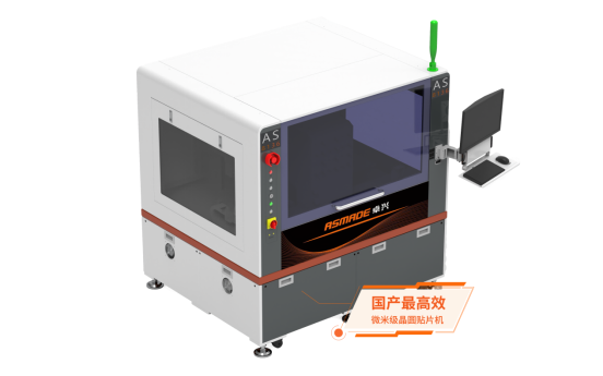
AS3606 Flip Chip Bonder | Zero Die Puncture Damage, Resolving Mass Production Bottlenecks of Micro LED MIP
2026-06-25(1)Browse
As chip sizes keep shrinking, PCB manufacturing faces surging difficulties and yield pressure, while traditional processes are trapped in dual challenges of precision and stability.
Core Pain Point of MIP Die Bonding: Massive Yield Loss Caused by Die Puncture Damage
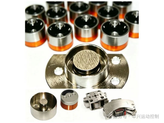
Ejector pins make direct contact with chip electrodes, leaving irreversible indentations that damage electrode structures and trigger electrical failure. With continuous miniaturization of dies, puncture-related defects account for 20%~30% of total die bonding defects. A large number of chips are scrapped due to damage. Conventional processes cannot eliminate this defect at the structural root, driving up production scrap costs and severely restricting product yield and long-term reliability.
Inherent Drawbacks of Two Traditional Die Bonding Processes
Traditional Solution 1: Front-side Die Bonding
· No built-in buffer protection structure. Full load of ejector pins acts directly on electrodes, easily causing electrode breakage and hidden lattice cracks inside dies.
· Such structural defects cannot be fully eliminated via parameter adjustment or consumable replacement, creating an unbreakable ceiling for mass production yield.
Traditional Solution 2: Needle Piercing Demolding
· High consumable cost: Custom UV release films are required, with four times the consumption rate of standard blue films, leading to high long-term material investment for mass production.
· Low equipment availability: Full parameter recalibration is mandatory for product changeovers, resulting in lengthy debugging cycles and production downtime that cuts effective output.
· Poor production scheduling flexibility: Incompatible with mixed production of multi-spec dies, requiring an extra pre-arrangement process and extending the overall manufacturing flow.
· Unstable mass production consistency: Tensile stress generated by demolding film shrinkage easily causes die warpage and offset, raising rates of subsequent cold solder joints and electrical failure.
Breakthrough Solution: Zhuoxing AS3606 Flip Chip Bonding Process – Zero Puncture Damage & Scalable Mass Production
Redesigned Force-Bearing Structure to Achieve Zero Puncture Damage Physically
On the basis of optimized pixel packaging structure, the equipment innovatively reshapes the force-bearing logic for die picking. The ejector pin bearing surface is shifted from electrodes to high-hardness sapphire substrates, which evenly disperse ejector pin pressure. Electrodes are completely isolated from mechanical compression, fundamentally eliminating electrode indentations, hidden die cracks, electrode deformation and other damages.

Full-Scope Mass Production Compatibility Advantages
Compatible with industry-standard blue films without modification to existing automated production lines. Equipped with single-arm exchange and non-stop material change architecture to shorten model switching time, supporting uninterrupted mass continuous production.
A multi-dimensional process comparison of front-side bonding, needle piercing demolding and flip chip bonding is shown below to intuitively reflect their comprehensive mass production differences.

Core Hardware Specifications of the Equipment

High-Precision Non-Destructive Pick-and-Place Unit
Positioning accuracy: ±15 μm; single machine throughput up to 45KUPH. Optional rigid and flexible ejector pins, with load applied only to the substrate layer, suitable for processing all specifications of micro dies.
High-Availability Flexible Mixed Bonding System
Supports non-stop material change for 6-inch wafer rings (customizable). Built-in angle pre-correction module. Compatible with simultaneous mixed bonding of 12 single-color rings and 5 RGB three-color rings, supporting multi-ring inline connection and multi-machine collaborative scheduling.
Full-Range Visual Inspection System
Covers full-process inspection of pick-and-place, die polarity and bonding positions. Equipped with XYθ submicron compensation function and automatic nozzle cleaning mechanism to continuously control mounting precision.
Full-Process Intelligent Connection Unit
Integrated substrate leveling, vacuum adsorption and side push mechanisms. Bidirectional assembly line connection to MES systems. Expandable with automatic loading/unloading robotic arms, optional laser height measurement, substrate and wafer ring scanning components.
Integrated Manufacturing System Compatible with Large Substrates
Synchronous Full-Array Die Bonding in Single Cabinet
Complete full-area pixel mounting within the shelf life of solder paste, maximizing the total number of pixels bonded in a single process and reducing process transfer times.
Ultra-Large Substrate Compatibility
Maximum support for 620×350 mm substrates, matching industry-standard 600×337.5 mm 16:9 display cabinets. No board splitting or segmented splicing required; complete single-cabinet full-board die bonding reduces multi-process transfer steps.
Upgraded Multi-Splicing Process for "Zero Splicing Gap" Production
Enables process upgrade from 24-splice to single-splice full boards, eliminating physical splicing gaps between cabinets and greatly improving picture integrity and fineness.

Traditional front-side bonding and needle piercing demolding processes fail to meet the demands of high yield, low cost and high-flexibility mass production, continuously hindering production line cost reduction and efficiency improvement. The Zhuoxing AS3606 flip chip bonder eliminates the core pain point of die puncture damage at the structural root, makes up for the deficiencies of needle piercing demolding in consumables, equipment availability, mixed production and product quality, and integrates the integrated ultra-large substrate manufacturing with zero splicing gaps. It empowers production lines to boost quality and cut costs in all dimensions, delivering a full advanced packaging solution for large-scale commercial mass production of MIP.
About Us
Shenzhen Zhuoxing Semiconductor Technology Co., Ltd. is a national-level "Little Giant" enterprise specializing in advanced packaging equipment and core semiconductor packaging technologies.
Founded by world-leading experts in motion control and packaging, the company boasts 20 years of profound technical accumulation and market implementation experience. Its core business covers new display, AI devices and PLP panel-level packaging equipment, alongside a complete product portfolio including power device packaging, intelligent control equipment and packaging process management systems.
Committed to providing global customers with one-stop, high-performance and highly reliable advanced packaging solutions, we are a high-tech enterprise integrating R&D, design, manufacturing, sales and technical services.
New Information
-
AS3606 Flip Chip Bonder | Zero Die Puncture Damage, Resolving Mass Production Bottlenecks of Micro LED MIP
We have conducted an in-depth analysis of the core pain poin...
-
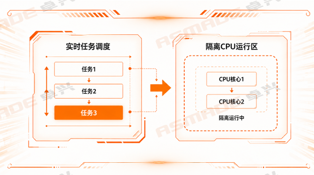
Real-Time Control with Standard C! Microsecond Hard Real-Time, Rapid Solution Deployment
This article introduces the AsMotion motion control solution...
-
AI Computing Power Surges: Domestic Micron-Level Die Bonder Solves High-Speed Optical Module Packaging Bottlenecks
Zhuoxing Semiconductor, a national‑level “Specialized, Sop...
-
For Precision Automation: High-Performance Lightweight Voice Coil Control Solution
Zhuoxing Semiconductor introduces a cutting-edge high-perfor...
0755-29691921
Hotline:0755-29691921
Phone:0755-29691921
Fax:0755-29691921
Email:market@asmade.cn
Address:Building 3, Xifengcheng Industrial Park, Fuhai Street, Bao'an District, Shenzhen City, Guangdong Province


 0755-29691921