Mini LED commercial launch in the first year, and Asmade Semiconductor flip chip COB solution may become an industry standard
2023-05-10(3606)Browse
In late April, the Mini LED industry ushered in heavy news: Apple released a new generation of iPad Pro on the 21st, and it was equipped with Mini LED backlight technology for the first time. One stone caused a thousand waves. This heavy news quickly ignited the upsurge of Mini LED technology. Well-known companies in the industry such as Asmade Semiconductor have expressed that Mini LED has officially entered the mass consumer market and ushered in a period of development opportunities. In 2021, it will be the Mini LED. The first year of LED commercial use.
Mini LED backlight technology is to upgrade the backlight area into countless independent small LED light sources. The backlight area of Apple ipadpro2021 is equipped with 10,000 small LED light sources, with 2,500 independent light control areas, which can display a pure black background. Compared with ordinary LCD The screen can be more transparent, the body can be thinner, and there will be no OLED burn-in and stroboscopic problems. It is precisely because of the excellent performance of Mini LED that it becomes a key link from LED to Micro LED. Many well-known companies in the industry have already made plans in advance. For example, Zhuoxing Semiconductor has taken the lead in laying out the Mini LED packaging process and providing a Mini LED flip-chip COB overall solution.
Judging from the data given by Apple, the initial performance of Mini LED is very impressive: the peak brightness has reached 1600nit, and the contrast ratio has reached 1 million: 1, which fully demonstrates the display performance of Mini LED. The reason why Mini LED is so good is due to its huge upgrade in technology. For example, the size of LED chips is on the micron level. There are usually thousands of chips and tens of thousands of solder points on each Mini LED circuit board to connect RGB three-color chip. Such a huge number of solder joints brings great difficulty to the packaging of the chip, and also puts forward higher requirements for the Mini LED packaging process.
Respond to every request! In response to the higher requirements of the Mini LED packaging process, Asmade Semiconductor has conducted special research on various aspects such as die bonding, testing, bonding, and repairing, and has given its own answer—the overall flip-chip COB packaging process solution.
Although flip-chip COB is the optimal solution for the current Mini LED packaging process, it puts forward higher requirements for the die bonder, which are mainly reflected in four aspects: precision, speed, substrate size and yield. Die bonding should be more precise, position error <±15um, angle error <1°; speed must be guaranteed before solder paste denatures; substrate width should be above 200mm; die bonding yield should be above 99.99%. At present, there are not many die bonders that can meet this demanding requirement. Asmade Semiconductor has provided solutions for these four points one by one by virtue of its professional background in the industry for many years.
Double insurance angle adjustment to ensure the accuracy of die bonding
To solve the problem of precision in the die-bonding process, Asmade Semiconductor has innovatively developed two sets of angle adjustment solutions. The first is to pass the correction of the wafer ring while the swing arm is grabbing the wafer to ensure that the swing arm grabbing correction is more accurate. Secondly, after the swing arm grabs the wafer, the angle of the wafer is adjusted to ensure that the wafer is fixed on the corresponding position on the substrate in a more standardized posture. Two angle adjustments, double insurance to ensure that the wafer position error and angle error are perfectly up to standard.
Solid crystal with both arms at the same time, speed is king
Because the timeliness of solder paste is an objective existence, the faster the die-bonding rate, the more LED chips per unit area, and the possibility of Mini LED or even Micro LED. Compared with the traditional double-arm double-plate die-bonding method, the number of die-bonding on the substrate per unit area will not increase, it is just a copy of the single-arm single-plate die-bonding method. To this end, Asmade Semiconductor has innovatively developed a dual-arm single-board simultaneous die-bonding, with two sets of swing-arm simultaneous die-bonding on a substrate per unit area, doubling the speed. More chips can be bonded before the solder paste is denatured. At present, the ASM3602 double-swing arm synchronous die bonder launched by Asmade Semiconductor can reach a bond speed of 40K/H.
Pressure control, side splitting and die bonding, the substrate can be larger
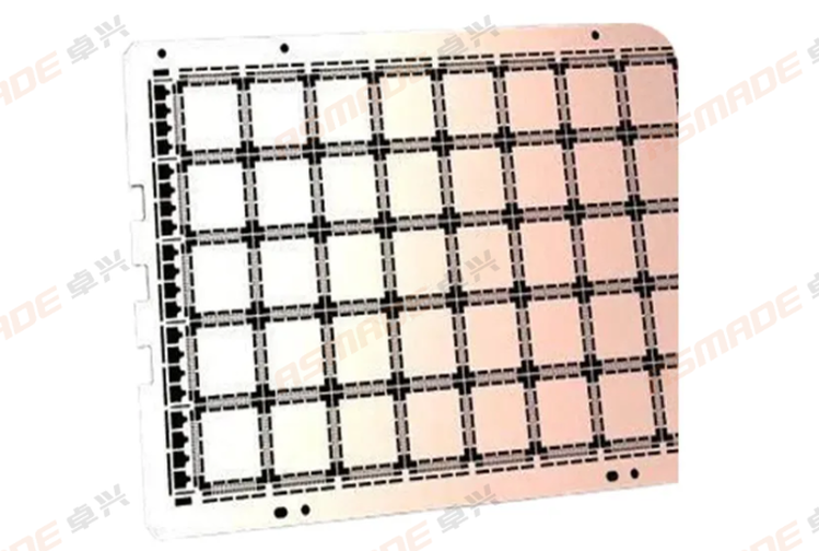
The Mini LED backlight technology is not only successfully applied to the Apple ipadpro 2021 this time, but also larger-sized applications such as TVs and computers will surely become a trend. If Mini LED wants to be larger in size, the substrate width must be greater than 200mm or greater. For this reason, Asmade Semiconductor has solved the problem that the substrate cannot be enlarged from two aspects. One is the dual-arm veneer die-bonding in two partitions at the same time, with the same arm length, partitioning the die-bonding can increase the width of the substrate; the other is pressure correction, through the adjustment of the pressure during die-bonding, it can meet the warping and unevenness of large substrates, and soft landing Guarantee the success rate of die bonding.
Multi-chip ring design, support for mixing and naturally high yield rate
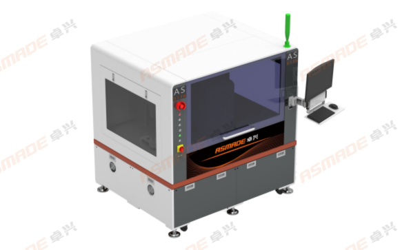
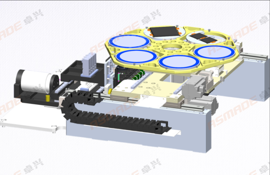
Only a high die-bonding yield rate can support the final display effect of Mini LED. Generally speaking, Mini LED’s requirement for die-bonding yield rate must be above 99.99%. In response to the requirements of Mini LED on the yield rate of die bonding, Asmade Semiconductor provided a multi-chip ring design and a mixed mode, and created a dual-arm 6-wafer ring ASM3603 COB die-bonding machine, which can realize RGB one-time use in one clamping Completed, mixed type can be used according to needs, ensuring the die bonding yield > 99.99%.
Apple's new-generation iPad Pro adopts Mini LED backlight technology for the first time, which promotes the rapid entry of Mini LED into the market. This is an opportunity for the Mini LED industry, and it also puts forward higher and more stringent technical requirements for participating companies. Science and technology is the primary productive force. Asmade Semiconductor always adheres to basic technology research and innovative research and development. It firmly believes that only by mastering the core key technologies can we obtain a stable track in the era of rapid development and leave our own in the development process of Mini LED. chapter.
New Information
-

You Are Cordially Invited | ASMADE Joins You at SEMICON China 2026 & electronica China
ASMADE, a leading provider of high-precision semiconductor e...
-

Technological Breakthrough! Chip-Level Printer Adds Three New Features
Zhuoxing Semiconductor has achieved a technological breakthr...
-

Multi-Process vs. Precision vs. Speed: How to Simultaneously Balance the Equipment
In the semiconductor packaging industry, the challenge of ba...
-

Automatic Ejector Needle Switching Technology | Solving Multi-Material Mixed Mounting Challenges
In semiconductor packaging processes, the challenge of multi...
0755-29691921
Hotline:0755-29691921
Phone:0755-29691921
Fax:0755-29691921
Email:market@asmade.cn
Address:Building 3, Xifengcheng Industrial Park, Fuhai Street, Bao'an District, Shenzhen City, Guangdong Province


 0755-29691921